A potentially lost art from the the early days of Microprocessor based computers.
What is it?
A PAL or GAL is a type of programmable logic gate chip whose basic design goal is to reduce the number of chips on a printed circuit board by allowing a designer to add truth tables to a single chip, thus reducing chip count.
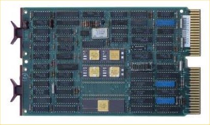
Typical board from the 70’s/80’s era… with lots of TTL Logic ‘glue’.
Boards can be made much smaller, or more dense by reducing the number of ‘black box’ types. In many cases, each of the smaller IC’s on the board above has a dedicated logic function that they offer one or more of. Basically, each chip is designed to perform one type of function.
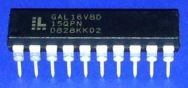
The PAL, or Programmable Array Logic, and GAL, or Generic Logic Array, are one-time and multi-use re-programmable logic IC that replaces many of these chips on the board. By allowing the logic decisions between inputs and outputs to be customized as needed, t
By today’s standards, these devices are obsolete as new devices have superseded them far more features and with pins numbering into the hundreds. The Complex PLD (CPLD) is well beyond what will be discussed here. They are programmed in an entirely different way than the legacy PLD devices. PLD’s are programmed in a way very similar to EPROMS and as a result, devices like the affordable TL866 programmer can be used to prepare them.
So, how would you use one of these? We can look at an example of where we can replace a few logic IC’s with a single chip. A good example is Grant Searle’s Z80 design. http://searle.hostei.com/grant/z80/SimpleZ80_32K.html
On the web page, there is a diagram of a small but complete Z80 based system. Some logic is used to route memory reads and writes as well as ROM address decoding and such.
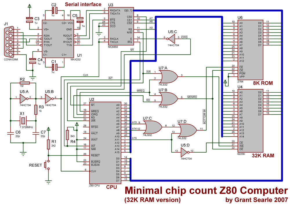
I’m talking about replacing U5 and U7 with a single chip. Keep in mind this is an exercise and was picked because it should be pretty easy.
So, if we look at what the chip is doing and how we can apply it to PLD design file…
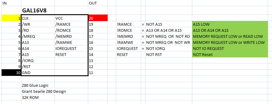
If you look at the equations on the right, you can see that this is what the 2 chips are accomplishing. (Ignore the system clock portion of U5) By carefully examining the logic of the wiring… this is what we ended up with.
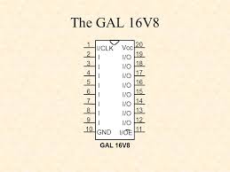
The nest step is to match the Inputs and Output pins to Names that are used in the equations.
The final step is to add the logic (far right column) equations into the programming file.
The resulting file looks like this:
Name     Z80MemDecode ;
PartNo   00 ;
Date     12/27/2018 ;
Revision 01 ;
Designer Pete Willard ;
Company  Personal ;
Assembly None ;
Location  ;
Device   G16V8 ;

/* *************** INPUT PINS *********************/
PIN 2   = !WR                     ; /*   WRITE                         */
PIN 3   = !RD                     ; /*   READ                          */
PIN 4   = !MREQ                   ; /*   MEMORY REQUEST                */
PIN 5   = A13                     ; /*   ADDRESS                       */
PIN 6   = A14                     ; /*   ..                            */
PIN 7   = A15                     ; /*   ..                            */
PIN 8   = !IORQ                   ; /*   INPUT OUTPUT REQUEST          */
PIN 9   = !RST                    ; /*   RESET                         */

/* *************** OUTPUT PINS *********************/
PIN 19  = !RAMCE                  ; /*  RAM Chip Enable                */
PIN 18  = !ROMCE                  ; /*  ROM Chip Enable                */
PIN 17  = !MEMRD                  ; /*  Memory  Read                   */
PIN 16  = !RAMWE                  ; /*  RAM Write                      */
PIN 15  = IOREQUEST               ; /*                                 */
PIN 14  = RESET                   ; /*                                 */

/* *************** LOGIC EQU  *********************/
RAMCE       = !A15                 ; /*                                 */
ROMCE       = A13 # A14 # A15      ; /*                                 */
MEMRD       = MREQ # RD            ; /*                                 */
RAMWE       = MREQ # WR            ; /*                                 */
IOREQUEST   = !IORQ                ; /*                                 */
RESET       = !RST                 ; /*                                 */
In order to program a
The editor used to create the specification (PLD) and JED file is called WINCUPL, which is a free tool made a available by ATMEL and still offered by the company acquired ATMEL, Microchip.
Here is the link: https://www.microchip.com/design-centers/programmable-logic/spld-cpld/tools/software/wincupl
So… DID IT WORK?
It turns out… WINCUPL has issues with NEGATIVE OUTPUT LOGIC in equations. So… back to the drawing board… I’ll provide a fix later…